Lab Proceedings[]
- Some further analogue FX pedal circuits were looked at and simulated
- The major project was discussed
Major Project[]
- The project talked about was a digital multi-FX pedal
- The basic layout discussed is as follows
Layout[]
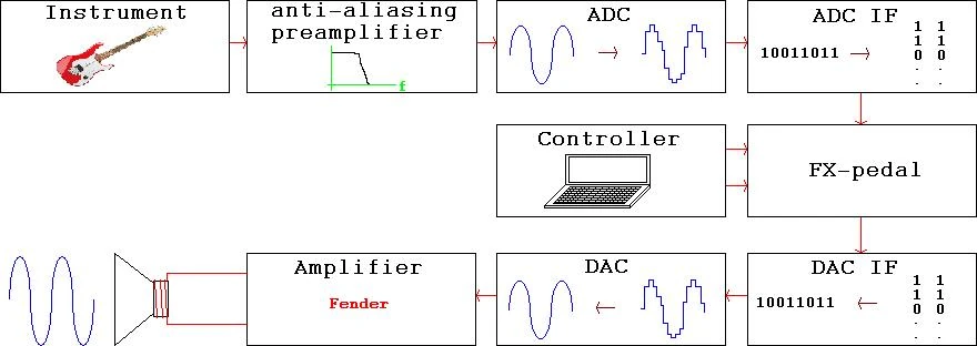
Instrument[]
The instrument can be modelled as a voltage source with a series resistance. Different instruments put out different voltage amplitudes. This can be tested in the lab and may become an important design parameter.
Preamplifier[]
The preamplifier serves two main roles:
- To amplify the signal to a level suitable for the input of the ADC. This requirement can be determined by reading the ADC data sheet.
- To filter the signal before sampling so that aliasing distortion is avoided. For more information, read wikipedia on the topics of sampling and aliasing. The sample rate is an important design parameter and would usually be around 44 kHz
Analogue-to-Digital Converter (ADC)[]
The ADC takes a sample of the input analogue waveform and translates it into serial binary data. Note that the ADC is already on the board, so we do not need to design one, just understand how the existing one works.
ADC Interface[]
The ADC interface takes serial data from the ADC and puts it in a form usable by the FX-pedal. Note that this is internal to our design and hence this is the first block that will need HDL coding. Also note that plenty of ADC manufacturers provide sample code for ADC interfaces; these may be used as a starting point when designing our system.
FX-pedal[]
This is our actual design. At first, this block will be simply an HDL module connecting the signals coming in from the ADC IF directly to the DAC IF. Once the other blocks are complete and a signal succesfully travels from the instrument, through the FPGA, to the speaker, work on the FX-pedal can start. This can be any sort of processing imaginable; a clipper for distortion, a flanger, a low frequency oscillator, the sky's the limit.
Contoller[]
This is the means used to control the functionality of the FX-pedal, i.e. to select which FX are used. In the spirit of keeping the intial design as simple as possible and adding complexity later, I propose making use of the on-board switches for this purpose. Later, a graphical user interface (GUI) may be designed.
DAC Inteface[]
The DAC interface takes parallel data from the FX-pedal and puts it in the serial form needed by the DAC. Note that this is internal to our design and hence will need HDL coding. Also note that plenty of DAC manufacturers provide sample code for DAC interfaces; these may be used as a starting point when designing our system.
Digital-to-Analogue Converter (DAC)[]
The DAC takes serial binary data and translates it into an analogue voltage. Note that the DAC is already on the board, so we do not need to design one, just understand how the existing one works.
Amplifier[]
At the moment the amplifier is a small Fender bass amp, with speaker included. However, this block may need additional design to condition the output of the DAC for the input of the amplifier. For example, the output voltages of the DAC may overdrive the amplifier and hence this signal will need to be reduced and a protection circuit will need to be built.
Architecture[]
The board to be used has not yet been decided upon. This is open for futher discussion based on price, features, and practical considerations like software tools (i.e. Xilinx would be better because UNSW have Xilinx tools installed).
The board suggested by me (pete) is the following one:
http://www.xilinx.com/products/devkits/HW-SPAR3E-SK-US-G.htm
It is relatively cheap, versatile, and has on-boars ADC and DACs
Design Methodology[]
The design methodology should be discussed in an effort to keep functional blocks consistent. This includes consideration such as which HDL to use, how to interconnect HDL modules, etc.