Circuit Diagram[]
Designers Description[]
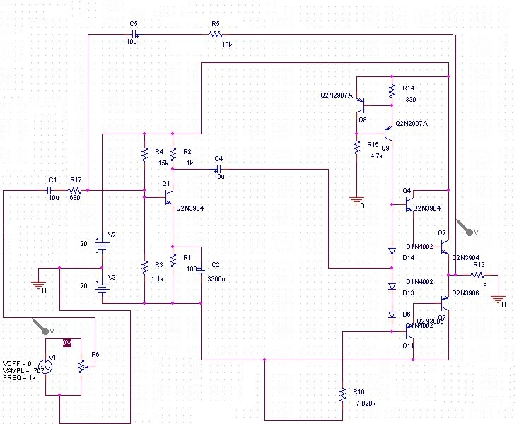
This amplifier uses a dual 20 Volt power supply and delivers 15 watts RMS into an 8 ohm load. Q1 operates in common emitter, the input signal being passed to the bias chain consisting of Q8, Q9, D6, D13 and D14. Q8 and Q9 provide a constant current through the bias chain to minimize distortion, the output stage formed by a discrete darlington pair (Q2,Q4) and (Q7,Q11). The last two transistors are power Transitors, specifically the 2N3055 and MJ2955. The 7.02K resistor, R16 was made using a series combination of a 4.7K, 680 Ohms, and two 820 Ohms. The 1.1K resistor, R3 was made using a 100 Ohms and a 1K resistor. You can use this circuit with any walkman or CD player since it is designed to take a standard 500mv RMS signal.
(Taken from http://www.zen22142.zen.co.uk/Circuits/Audio/amp15.htm)
Overall Description (by Peter Oliver)[]
I don't guarantee that anything I say is correct: The input signal is applied via V1 and is immediately applied to a potentiometer which takes a proportion of the input signal (i.e. volume control). V2 and V3 are the 20V DC sources which power the amplifier. The signal is then coupled via C1 to block DC. C1 is quite large so that only very low frequencies see it as a big impedance. AC sees C1 as a short circuit (approximately) hence the signal flows via R1 into the base of Q1.
R1 is needed to limit the current flowing into the base. Q1 is biased using the voltage divider R4 and R3 hence an operating point of about 2.7 V is setup, about which the signal can swing. Q1 operates in common-emitter mode, with its output flowing into C4. This particular transistor can drive about 200mV.
R1 acts as an element of negative feedback, which acts to stabilise the DC bias conditions and reduces the gain of this stage of the amplifier, this sacrifice in gain serves to increase the bandwidth of the amplifier and also to make the gain of this stage highly dependent on the resistor values as opposed to the gain of the transistor, which is unpredictable and varies with temperature. The increase in bandwidth, as well as the gain of this stage, can be found by finding the feedback factor, which can be found by performing small signal analysis, covered in ELEC2133. It is not intended for R1 to affect the AC signal at the output of this stage, it is there to stablise the DC conditions. Therefore C2 is included, which is known as a "by-pass" capacitor. It is very large and hence will only impede extremely low frequencies and DC (i.e. at f = 20Hz the impedance = 1/j*2*Pi*f*C = 3.6 Ohms!), to most AC it creates a short circuit across Q1, hence we have the traditional common-emmiter amplifier.
The output voltage swing is quite large now and ready to drive the power stage. Like C1, C4 AC couples to the next stage, i.e. blocks DC. The power stage operates in class AB mode. This means that the output is driven by two transistors in a push-pull configuration that are only just conducting, due to their bias arrangments. This arrangment has a little bit more distortion than a common-emmitter configuration (i.e. the first part of this amplifier), however it is far more efficient and as can be seen from the diagram, there is no resistor in the final output stage (appart from the 8 Ohm which is actually our speaker). Such a resistor would have to be rated at about 15 watts (BULKY) and would have to dissipate a heap of power (heat sink, fan).
The power transistors Q4, Q2 and Q11, Q7 are arranged in a darlington pair configuration in order to bump the current right up. Q8 and Q9 create a constant current source which flows through the diodes and R16 to ground. This has the effect of making sure that Q4 and Q11 don't turn off and are always at least just on which avoids the distortion created by transistor switching transisents and cross-over distortion. In the positive half cycle, Q2 drives current through the load, while in the negative half cycle, Q7 drives the load.
R5 is another feedback element with the same benefits mentioned above. C5 AC couples this path to avoid upsetting DC operating conditions.